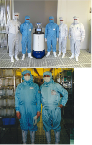
Biography of Principal - Douglas Pike
|
Doug is a very experienced semiconductor engineering professional. He is a veteran of silicon valley and has worked at five major companies during his varied career. He has
been a manager at every phase of silicon wafer fabrication engineering and manufacturing and came up through the ranks of process engineering, design engineering, process development and yield enhancement engineering to become Wafer Fab Director. ExperienceHis career includes experience with all major silicon process technologies including MEMS, Bipolar, CMOS, BiCMOS, DMOS, IGBT and DI.
He has been involved in start up companies for MEMS, Power MOSFETs, IGBT's and Optoelectronics. He has expertise in yield engineering and failure analysis of circuits from MEMS, Bipolar, Bipolar Opto, CMOS, BiCMOS, IGBT and power DMOS. EducationHe received the MSEE and BSEE degrees from Lehigh University in Bethlehem, PA where he studied with Dr Frank Hielscher in Microelectronics.
PatentsHas 13 patents in areas such as circuit design, process flow and process architecture
Project SummaryProcess Architecture
|
Process Development
- Transparent conductive film development, utilized in optical devices as electrical noise shield.
- Reactive sputtering, noble metal barrier and liftoff technologies developed
- Photoresist planarization developed and utilized to produce one of the industry's standard DMOS technologies
- Platinum evaporation or sputtering developed to obtain excellent switching speed for power IGBTs and diodes
Yield Improvement
- Arsenic Implant Annealing to solve junction leakage problem
Mobile: (541) 420-1243
dapike@dapikeengineering.com
https://www.linkedin.com/company/dapike-engineering-inc
dapike@dapikeengineering.com
https://www.linkedin.com/company/dapike-engineering-inc

